High-Reliability Membrane Switches & Tactile Arrays
Manufactured under ISO 9001 certified cleanroom environments, tested to over 1,000,000 actuations, and delivered with rapid air-freight logistics straight to San Francisco, San Jose, and Oakland production lines.
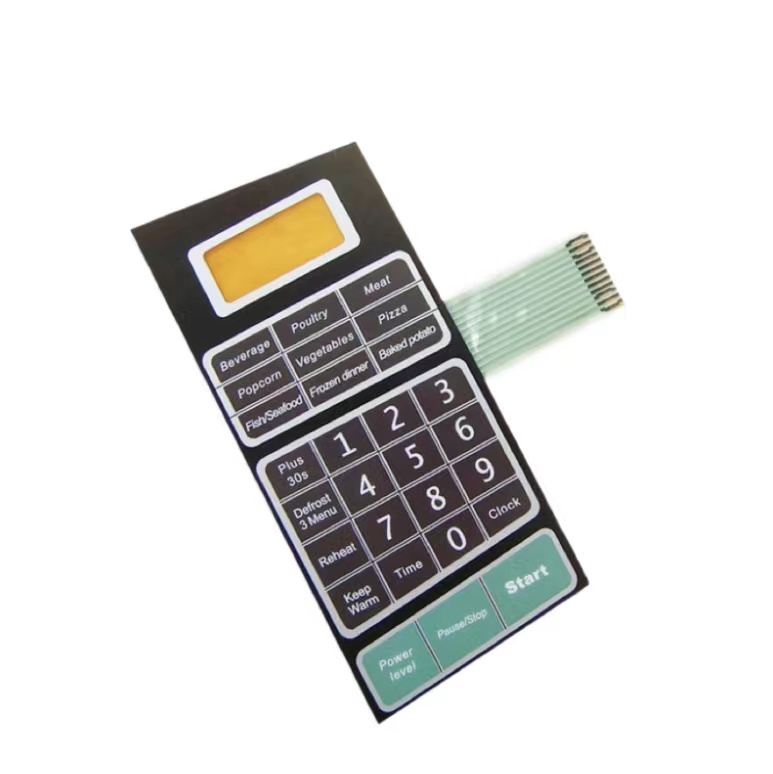
Low MOQ Custom Membrane Switch Panel Keypad Control
- Substrate: Autotex Hardcoated PET
- Actuation: Tactile Metal Dome (300g)
- Tail Type: 0.5mm / 1.0mm Pitch FPC
- Prototype MOQ: Starting from 10 pcs
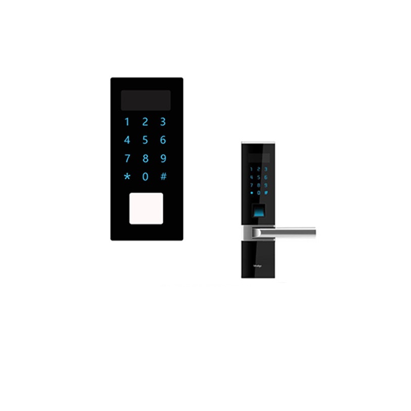
Custom Waterproof Keypad Smart Door PMMA Membrane Switch Panel
- Front Facia: Optical Grade Acrylic (PMMA)
- Ingress Level: IP67 / IP68 Continuous Seal
- Electronics: Capacitive Sensing Bus
- Application: Biotech Lab / Cleanroom

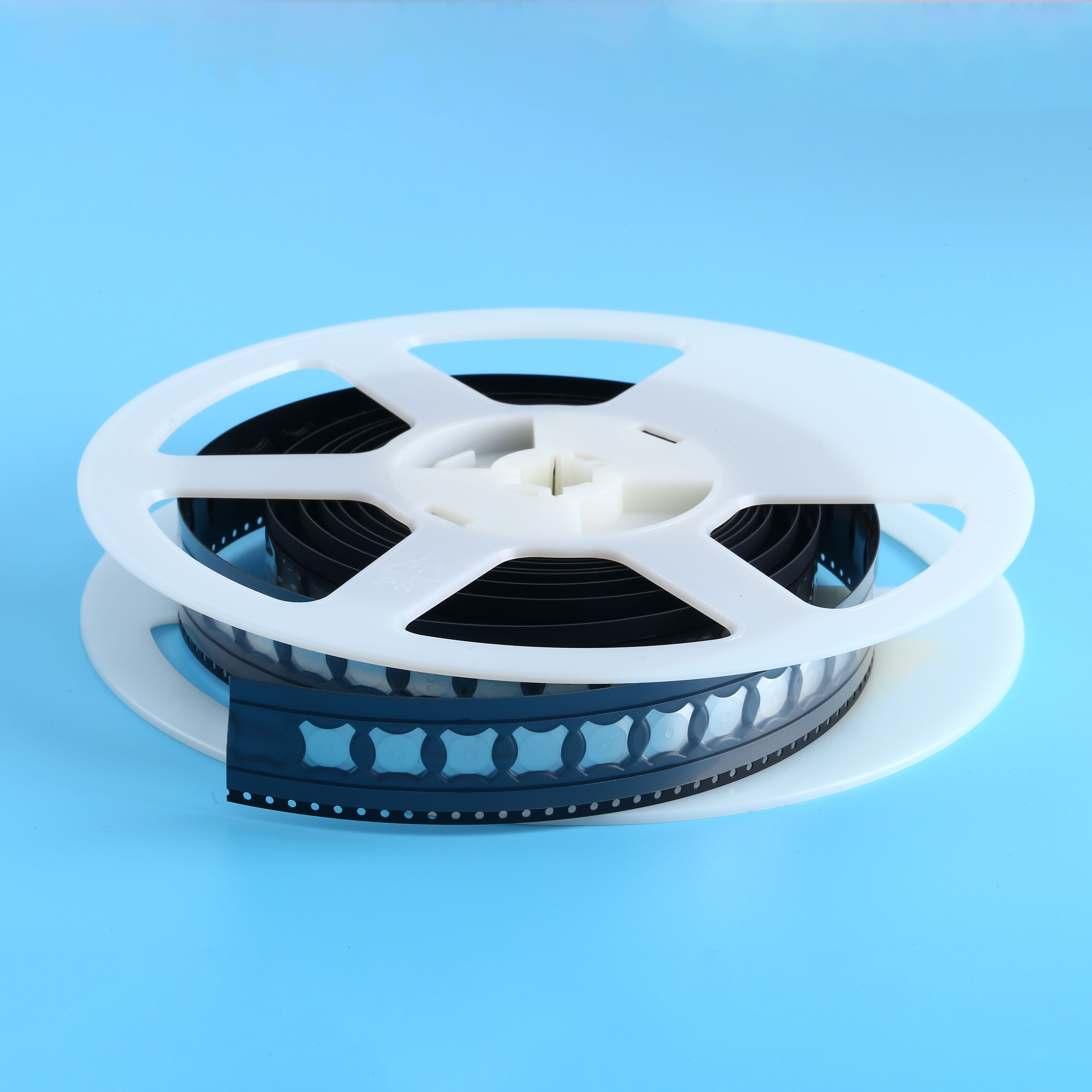
SMT Cross 4-Legged Snap Dome in Reel Packing
- Configuration: 4-Leg Cross with Dimple
- Packaging: Tape & Reel for Auto Pick-and-Place
- Plating: Nickel / Gold Contact Layers
- Operating Life: >1,000,000 Cycles
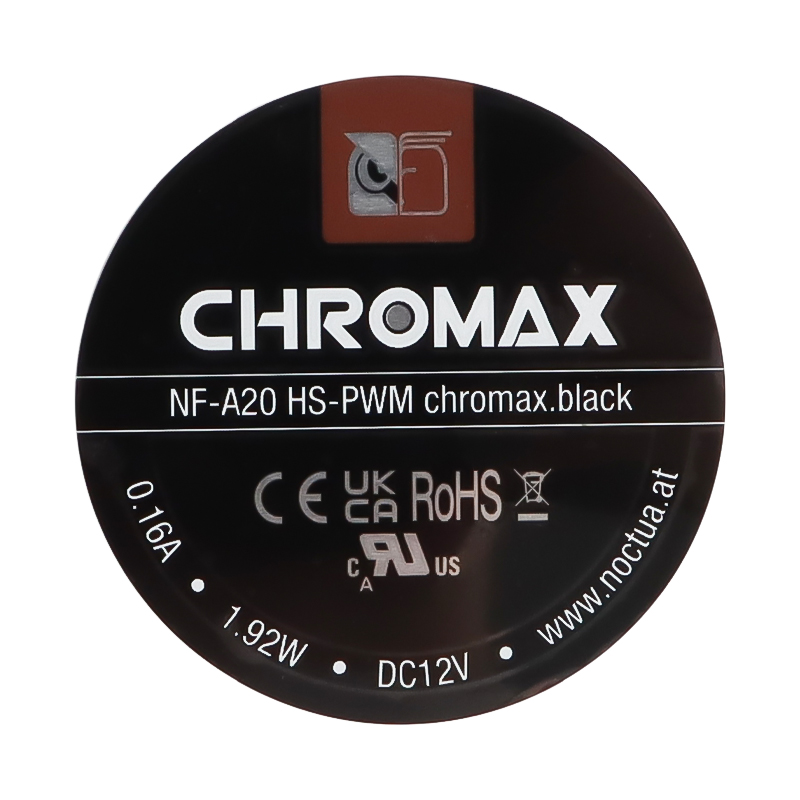
Customized Laser Engraved Metal Crafts Nameplate
- Alloy: AISI 304/316 Stainless Steel & AL
- Process: Fiber Laser Vector Engraving
- Adhesive: 3M 468MP High Shear Bond
- Durability: Solvent, Acid & UV Proof
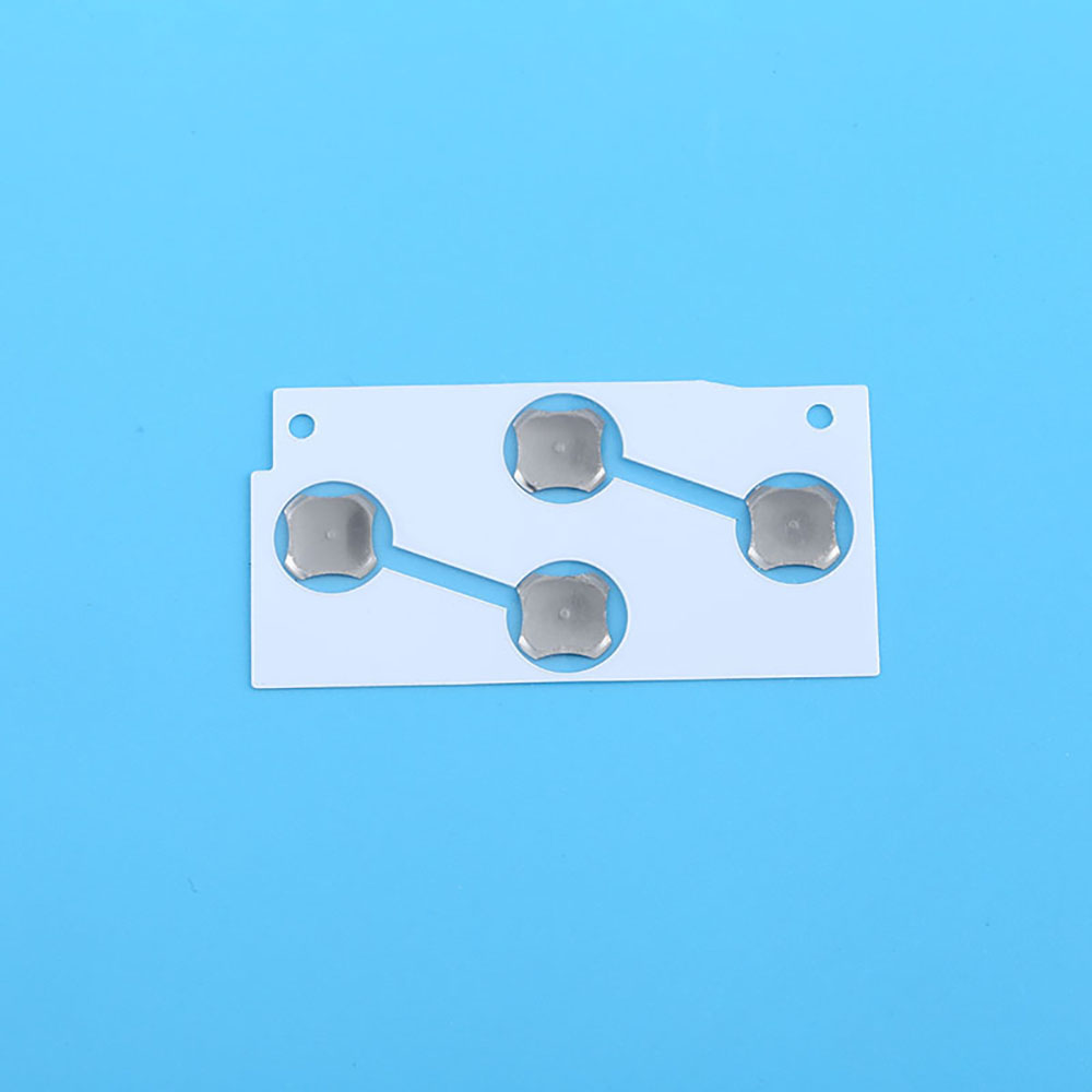
Customized Metal Dome Array Multi-Key Matrix
- Layer Setup: Adhesive PET Carrier Sheet
- Dome Diameters: 6.0mm, 8.4mm, 10.0mm, 12.0mm
- Venting: Internal Micro-Air Escape Channels
- Assembly: Peel-and-Stick Quick Mount
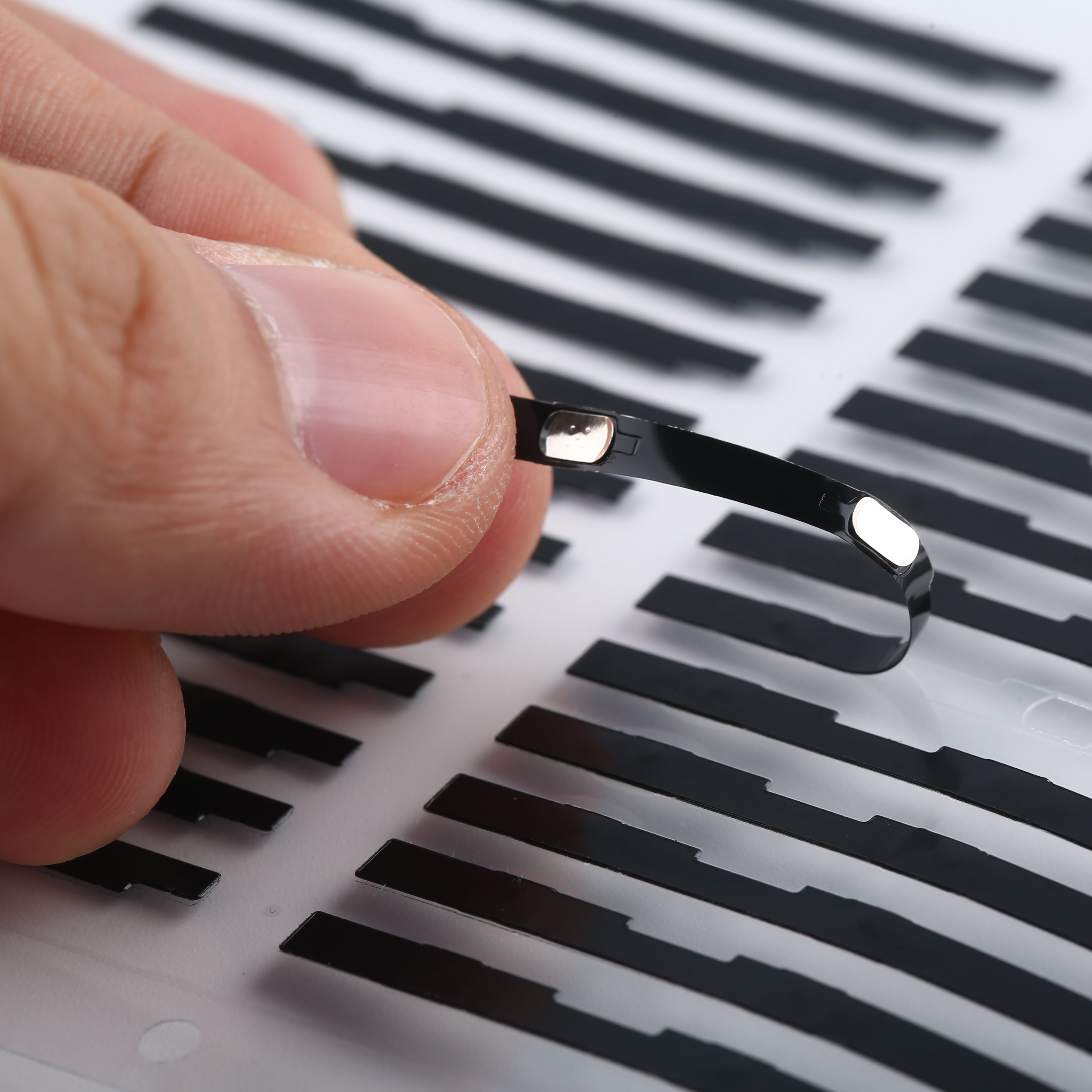
Oval Metal Dome Array Single Layer PET with Adhesive
- Geometry: Oblong / Oval Snap Geometry
- Tactile Ratio: > 50% Crisp Snap Feedback
- Profile: Ultra-Low Height (<0.35mm)
- Usage: Wearables & Handheld Peripherals
Transparent PET Metal Dome Array for Control Keypads
- Backer: High-Clarity Optical PET Film
- Dome Shape: Round Contact Dimple (180g-350g)
- Circuit Compatibility: Rigid FR4 & Flexible Polyimide
- Resistance: Contact < 1.0 Ohm
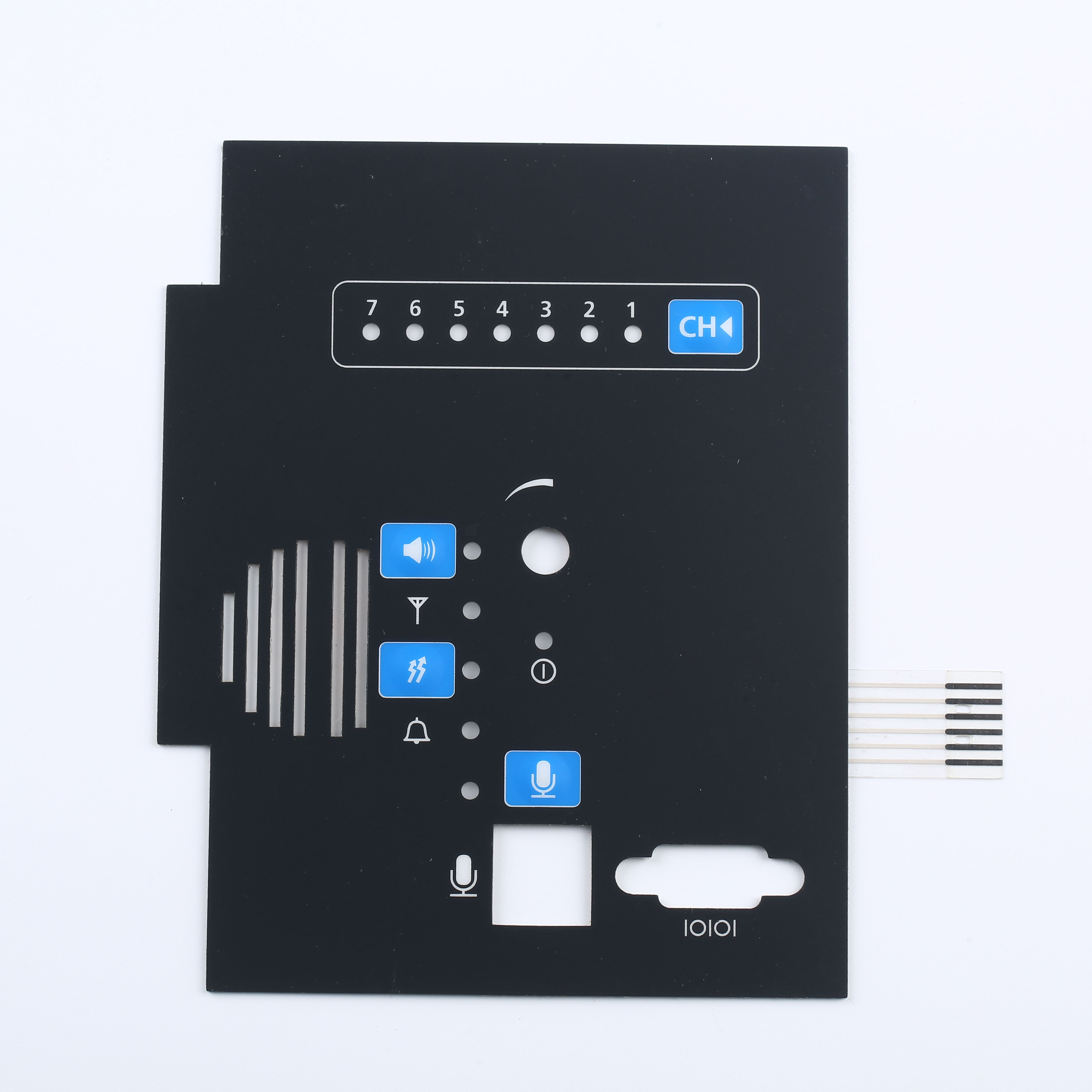
Polycarbonate Film Screen Printing Instrument Panel
- Material: Lexan™ Polycarbonate (0.175 - 0.5mm)
- Display Windows: Dead-Front / Transparent Filter
- Embossing: Pillow / Rim Tactile Perimeter
- Printing: Subsurface Reverse Screen Print
Serving the Greater San Francisco & Silicon Valley Hardware Corridor
From biotech cleanrooms in South San Francisco to autonomous robotics labs in Berkeley and Fremont EV manufacturing lines, our engineered human-machine interface (HMI) panels solve mission-critical operational challenges.
South SF Biotech & Clinical Diagnostics
San Francisco and the Peninsula host the world's most concentrated life sciences ecosystem. Centrifuges, DNA synthesizers, blood analyzers, and surgical automation consoles demand continuous surface sanitization.
- Antimicrobial Overlay Films: Polyester treated with micro-silver ions preventing pathogen growth.
- Chemical Resistance: Impervious to aggressive wipe-downs using isopropyl alcohol (IPA), bleach (sodium hypochlorite), and Cidex.
- True IP67 Hermetic Sealing: Solid perimeter perimeter gaskets prevent reagent leakage into switch circuitry.
East Bay Robotics & Autonomous Logistics
Autonomous mobile robots (AMRs) and industrial handling units developed in Fremont, Hayward, and Richmond require robust physical emergency inputs and tactile human interaction in harsh warehouse environments.
- High Tactile Snap Ratio: 4-leg metal snap domes providing positive mechanical confirmation through operator gloves.
- Polyurethane Armor Coating: Thick cast PU resin keytops protecting against heavy abrasive wear and tool impacts.
- Wide Thermal Range: Stable operation from -40°C deep freeze storage up to +85°C industrial transport racks.
Silicon Valley CleanTech & EV Charging
The transition toward electric transportation infrastructure across Northern California requires outdoor EVSE chargers, solar inverter interfaces, and battery telemetry units engineered for continuous environmental exposure.
- UV-Stabilized Weathering: Autotex XE exterior-grade PET film rated for over 10 years of direct California solar radiation without yellowing or embrittlement.
- EMI / RFI Shielding: Printed aluminum foil or selective carbon/silver mesh grounding to suppress high-voltage inverter switching noise.
- Condensation Venting: Engineered hydrophobic membranes preventing internal pressure distortion during coastal fog swings.
Emerging Design Trends in San Francisco Hardware Startups
Modern hardware teams across the Bay Area are shifting away from clunky mechanical assemblies toward integrated thin-profile interface modules. Here are the core specifications driving hardware engineering RFQs today.
1. Capacitive Touch & Tactile Metal Dome Hybrid Integration
Silicon Valley consumer and industrial electronics designers increasingly demand the sleek appearance of smooth touchscreen glass paired with the zero-fail tactile feedback of mechanical metal snap domes. Cevra engineers hybrid panels where non-critical navigation uses projected capacitive touch traces printed on thin film, while critical activation buttons (Power, Start, Emergency Stop) leverage physical stainless steel domes mounted beneath embossed graphical relief.
2. Ultra-Thin Light Guide Film (LGF) Uniform Backlighting
Bulky legacy light pipes and discrete point-source LEDs are being replaced by micro-etched Light Guide Films (LGF). With overall thicknesses under 0.25mm, LGF utilizes side-firing ultra-compact SMD LEDs mounted directly on the circuit layer. Specialized micro-dots refract light upward uniformly across switch legends, icon perimeters, and company logos, eliminating hotspots while reducing standby battery drain on portable Bay Area IoT field monitors.
3. Silver Migration Prevention via Carbon Passivation
San Francisco's high maritime humidity coupled with DC electrical bias can induce silver dendritic growth (silver migration) across fine trace paths, resulting in intermittent short-circuits. Cevra protects circuit integrity by over-printing conductive silver traces with high-density carbon conductive paste (passivation layer), locking silver molecules in place and preventing ionization even under continuous 85°C / 85% RH accelerated life testing.
4. ESD Shielding to 15kV Discharge Thresholds
Dry office conditions and industrial factory floors in Silicon Valley frequently generate severe electrostatic discharge (ESD). Without proper perimeter and face shielding, ESD arcs can jump through the graphic overlay directly to sensitive microcontroller logic on the customer's mainboard. Our panels integrate continuous printed aluminum, silver grid, or copper mesh shields capable of shunting air discharges up to 15kV directly to chassis ground.
Graphic Overlay & Substrate Selection Guide
Selecting the proper substrate determines switch life expectancy, chemical resistance, and optical transmission. Review the engineering properties below to optimize your bill of materials (BOM).
| Engineering Parameter | Autotex Biaxially Oriented PET | Lexan Optical Polycarbonate (PC) | PMMA Acrylic Facia Plate |
|---|---|---|---|
| Mechanical Flex Life | > 5,000,000 switch actuations | ~ 100,000 to 200,000 cycles | Rigid (non-flexing front plate) |
| Chemical / Solvent Resistance | Exceptional (IPA, MEK, bleach, detergents) | Moderate (attacked by aromatic solvents) | High resistance to acids and bases |
| Embossing Retention | Permanent shape retention at 85°C | Crisp initial form; susceptible to stress relaxation | N/A (flat, machined or CNC step-beveled) |
| Surface Hardness Rating | 2H to 3H pencil hardness | 1B to 1H (requires UV hardcoat) | Up to 4H to 6H scratch resistance |
| Optical Window Transmission | > 90% (anti-glare / gloss textures) | > 92% (high clarity for OLED/LCD) | > 94% (crystal clear optical grade) |
| Optimal Application Space | Medical diagnostics, industrial AMRs, oil & gas | Consumer devices, decorative backplanes | Touchscreen overlays, smart appliances |
Tactile Snap Ratio Formula: Engineering the "Click" Feel
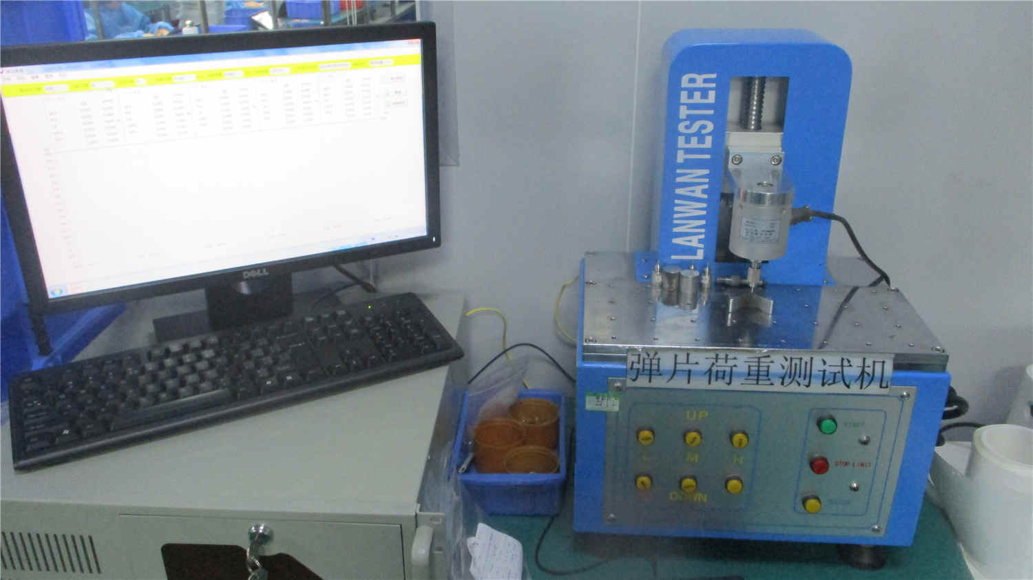
Our mechanical engineers calibrate tactile feel using precision dome load displacement testers: Click Ratio (%) = [(Actuation Force F1 − Contact Force F2) / Actuation Force F1] × 100%. For San Francisco medical devices, we engineer a subtle, low-noise click ratio of 35% to 45% (F1 = 220g). For heavy robotics and outdoor construction controllers, we dial in an aggressive, high-feedback snap ratio of 55% to 65% (F1 = 350g to 450g) to guarantee confirmation even through heavy insulated gloves.
Dongguan Cevra: Verified In-House Manufacturing Strength
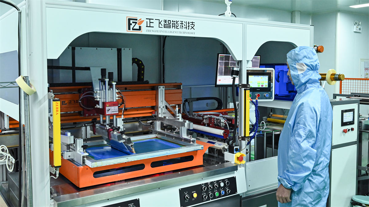
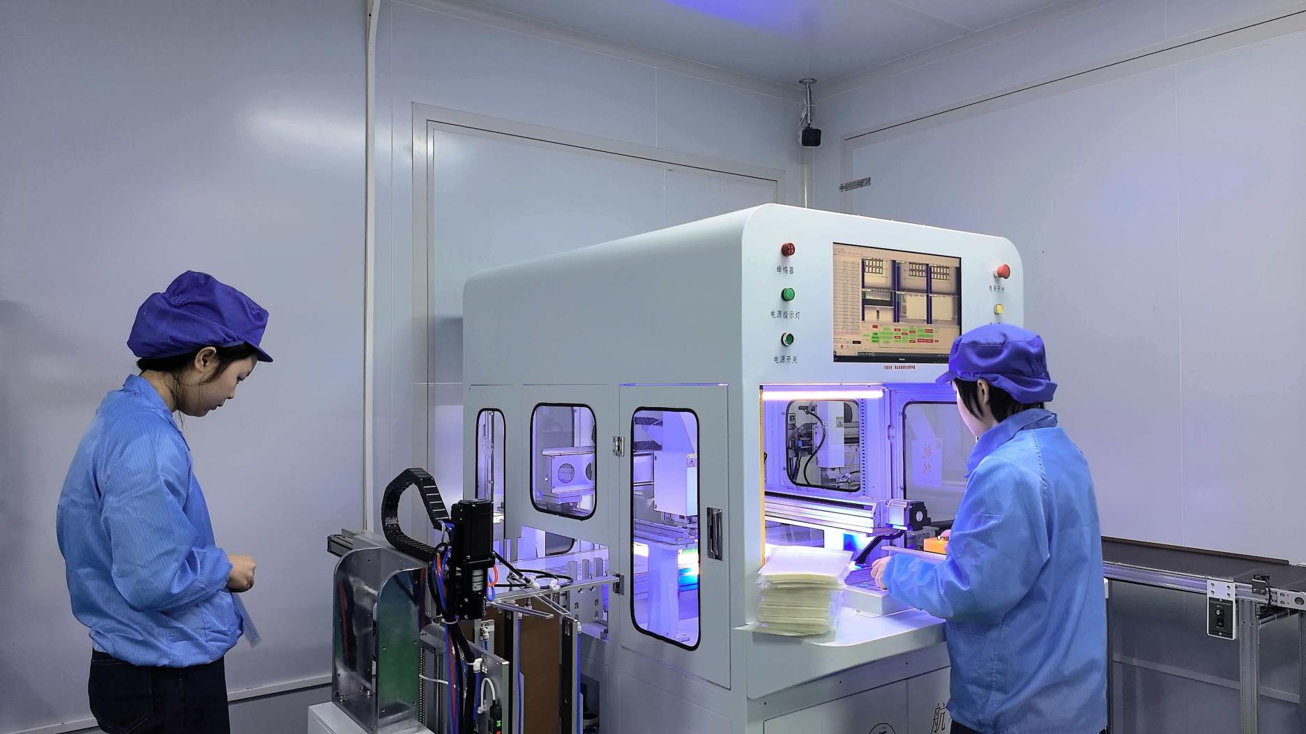
Unlike trading entities, Cevra operates a dedicated 2,600m² manufacturing facility established in March 2009. We manage the entire fabrication lifecycle from raw substrate slitting to cleanroom automated lamination under one certified roof.
Full In-House Fabrication Chain
We execute 100% of production processes internally: semi-automatic precision screen printing, CCD visual targeting drill presses, CNC die-cutting, laser kiss-cutting, automatic laminating, and robotic snap dome placement lines. This guarantees tight dimensional tolerances (±0.05mm) and immediate turnarounds on design revisions.
Comprehensive Laboratory Testing
Every lot undergoes stringent mechanical and environmental verification: computer-controlled dome actuation curve testers, 180° peel adhesion testers, constant holding tack gauges, electric pencil hardness testers (ASTM D3363), and high/low thermal shock cabinets (-40°C to +125°C) to withstand rugged Bay Area field deployments.
Seamless Pacific Supply Chain
Located in Dongguan—the epicenter of global electronics hardware—we leverage direct daily flights into San Francisco International (SFO) and Oakland International (OAK). Custom prototypes ship in 5 to 7 business days, enabling agile hardware sprints for accelerator startups in Y-Combinator, hardware incubators, and established OEM giants alike.
Frequently Asked Questions by San Francisco Bay Area Buyers
Clear, direct answers regarding prototype lead times, international freight options to California, DFM design files, and regulatory compliance.
How fast can Cevra deliver custom functional prototypes to San Francisco?
Our standard prototype cycle is 5 to 7 business days following final artwork sign-off and layer stack approval. By utilizing rapid laser cutting instead of hard tooling for initial samples, we eliminate tooling lead times. Prototypes are dispatched via DHL Express, FedEx Priority, or UPS Worldwide with transit times of 2 to 4 days directly to your facility in San Francisco, San Jose, or Sunnyvale.
What engineering design files are required for DFM (Design for Manufacturability) review?
We prefer vector-based files such as Adobe Illustrator (.AI), vector PDF, or AutoCAD (.DXF / .DWG) for graphic overlays and cut profiles. For internal silver or flexible FPC circuit layers, Gerber files or native Altium/CAD layout files are welcomed. Our engineering team provides a complimentary DFM analysis within 24 hours, reviewing minimum trace spacing (0.35mm recommended), venting channel paths, tail bend radii, and adhesive border tolerances.
How do you prevent moisture ingress in outdoor coastal environments like the SF Bay?
San Francisco's microclimates feature heavy coastal fog, morning condensation, and salt air. To achieve genuine IP65, IP67, or NEMA 4X seals, we engineer complete perimeter gaskets using 3M 300LSE or 3M 467MP/468MP acrylic adhesives. Tail exits are designed with silicone compound sealing barriers or custom rear-exiting FPC routings that isolate conductive contacts completely from ambient humidity.
Are Cevra membrane switch materials compliant with RoHS, REACH, and California Proposition 65?
Yes. All raw materials—including polyester substrates (Autotex, Melinex), conductive silver and carbon inks, adhesives (3M, Nitto), LEDs, and connectors—strictly conform to EU RoHS Directive 2011/65/EU, REACH regulations, and California Proposition 65 chemical disclosure thresholds. Full certificates of compliance (CoC) and third-party laboratory test reports are provided with every production run.
What is your minimum order quantity (MOQ) for custom hardware startups?
We actively support seed-stage and Series A hardware incubators across the Bay Area. Prototype batches start as low as 10 to 50 pieces. As your product scales to Pilot Production and Volume Commercial Distribution, our 2,600m² facility easily accommodates ramp-ups to 100,000+ units per month with high-volume price tier discounts.
Can you execute a bilateral Non-Disclosure Agreement (NDA) prior to receiving proprietary CAD?
Absolutely. We routinely sign standard mutual NDAs with Bay Area venture-backed firms, medical device inventors, and defense robotics integrators before reviewing any proprietary CAD or intellectual property. Your industrial designs and circuit schematics are stored on encrypted internal servers and never shared with external third parties.
Accelerate Your HMI Project with a Direct Manufacturer
Send us your artwork, CAD drawings, or engineering specifications. Our senior HMI engineers will provide a comprehensive DFM manufacturability review, material recommendations, and a competitive factory quotation within 24 hours.