Engineered Membrane Switches, Dome Arrays & Backlit Controls
Direct OEM/ODM production verified to ISO 9001:2015. Tailored for rugged integration with precision optical light guides, backplanes, and tactile interface consoles.
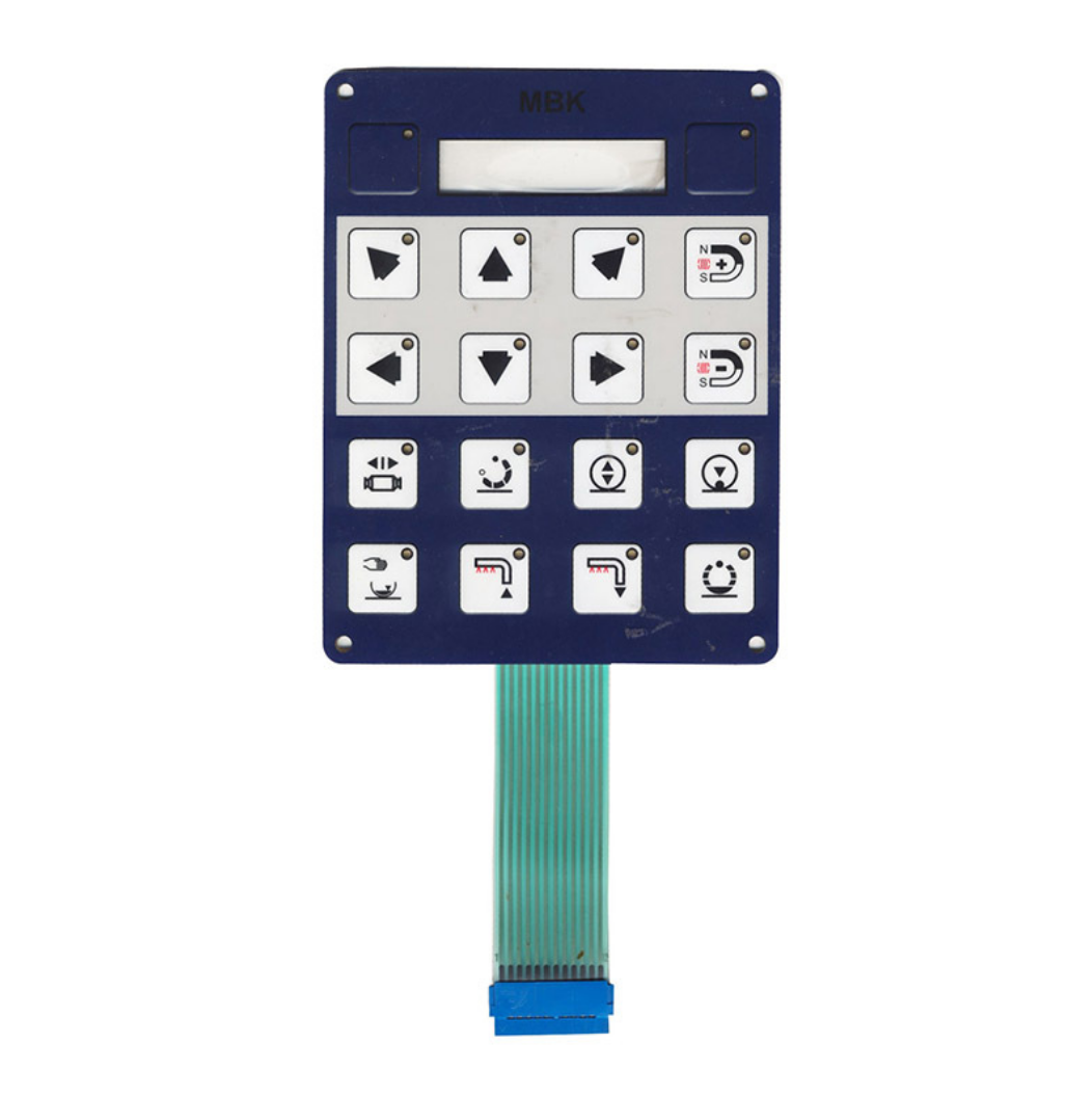
- Layout1 Row × 4 Keys
- SubstratePolyester / PET
- Tactile FeelCrisp Snap Dome
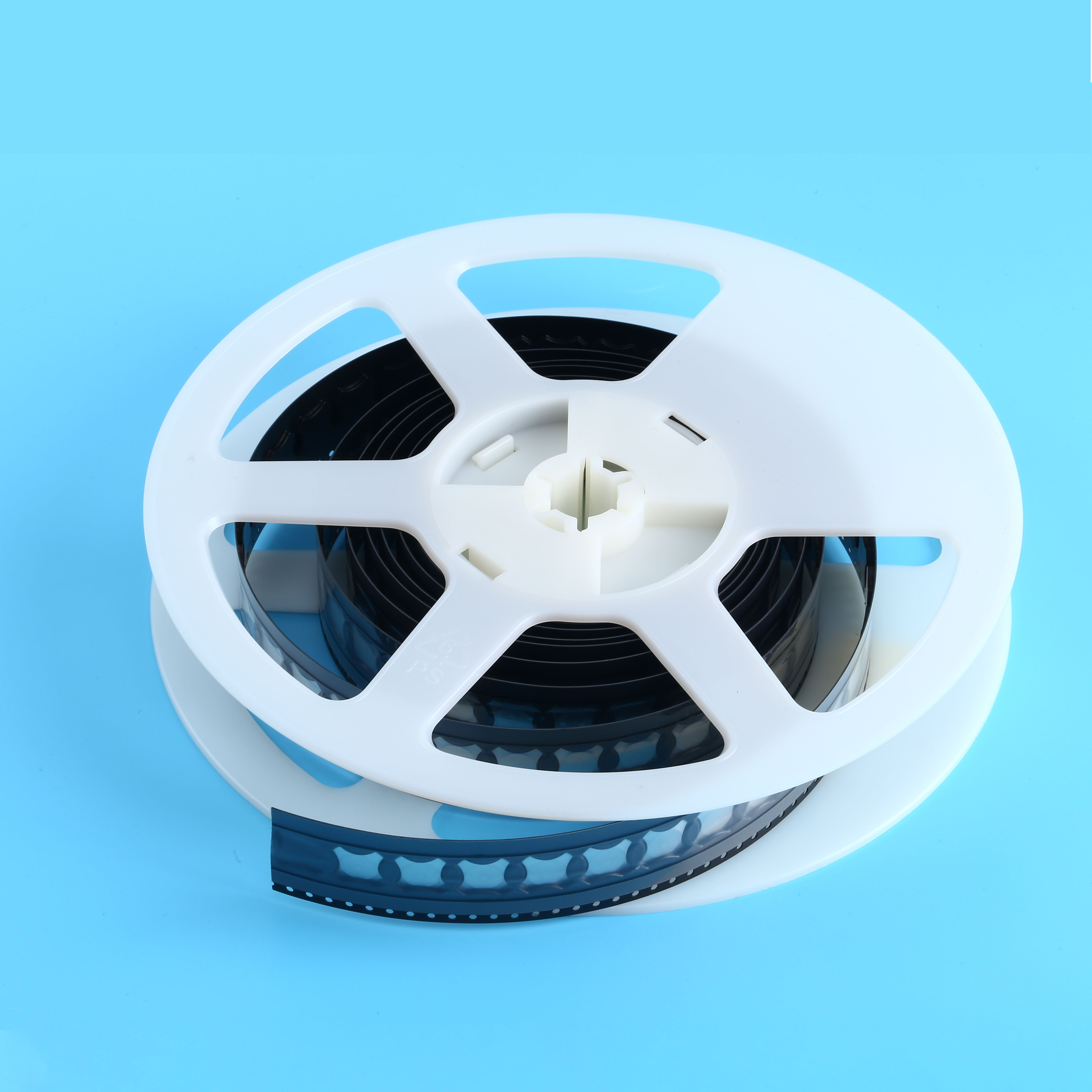
- Configuration4-Leg Cross / Dimpled
- PackagingReel Packing / Tape
- Life Cycle> 1,000,000 Actuations
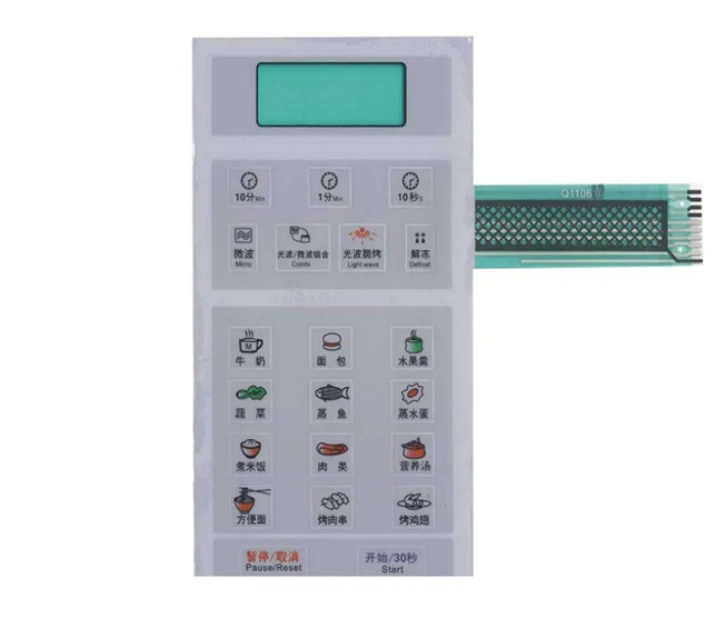
- SealingIP65 / NEMA 4 Rated
- Circuit TraceConductive Silver / Carbon
- TerminationStandard Pitch Tail
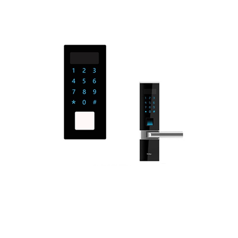
- Front PanelOptical Grade PMMA
- Touch ModeCapacitive Sensing
- Ingress RatingWaterproof IP67
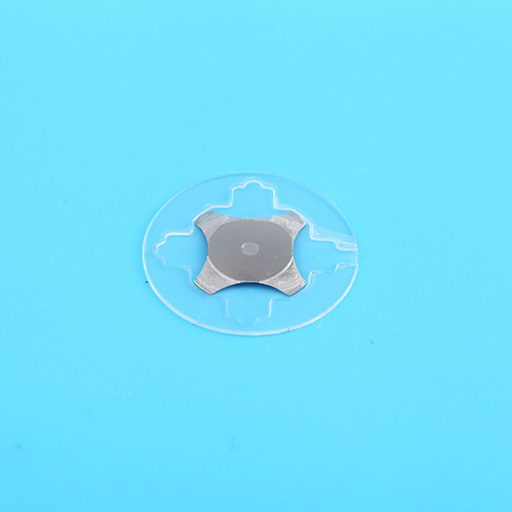
- Adhesive LayerHigh Tack 3M / PET
- Dome PlatingNickel / Optional Gold
- AssemblySelf-Aligning Carrier
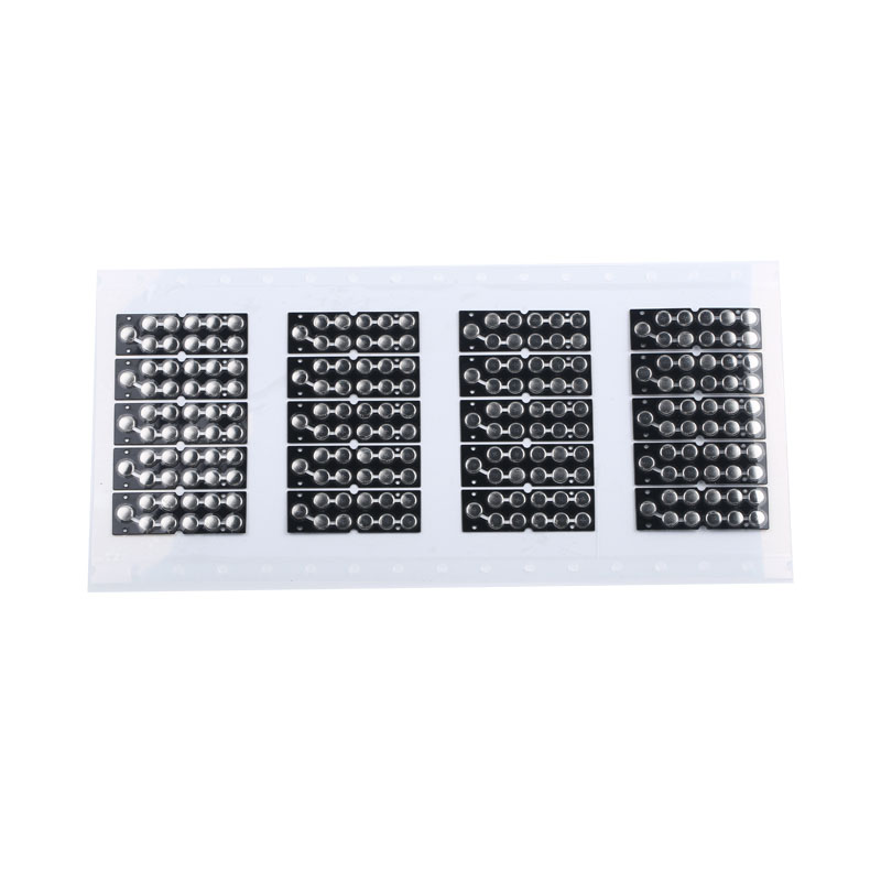
- Dome GeometryCircular Snap Dome
- Carrier FilmClear Optical PET
- Actuation Force160g – 350g Customized
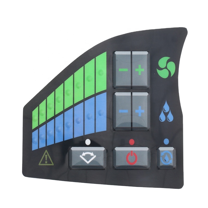
- PrintingHigh-Density Silk Screen
- Key FinishingRim / Pillow Embossing
- Lighting OptionLGF / Backlit Windows
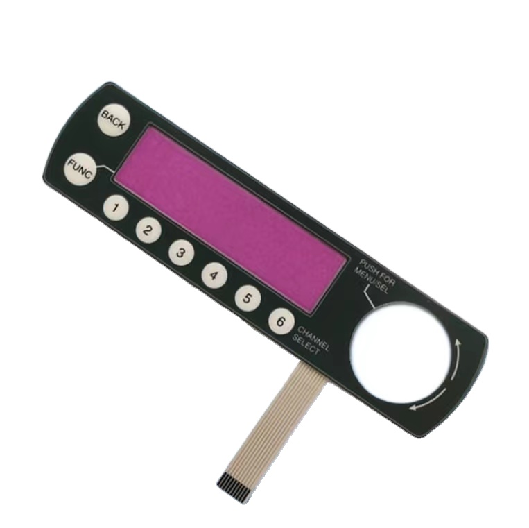
- SanitizationChemical / IPA Resistant
- ComplianceClass 10,000 Cleanroom Built
- CircuitMulti-Layer Silver Conductive
Technical Deep-Dive: Light Guide Plate (LGP) Engineering for Boston Hardware Innovators
The Greater Boston hardware ecosystem—anchored by elite robotics research in Cambridge, medical device clusters along Route 128 (Waltham, Woburn, Burlington), and biotechnology incubators in the Seaport District—demands extreme optoelectronic performance. An LED Light Guide Plate (LGP) or Light Guide Film (LGF) is fundamentally an optical-grade polymer substrate engineered to convert point-source or linear-source edge-lit LEDs into a perfectly uniform, planar light surface via Total Internal Reflection (TIR).
Achieving uniform luminance across large surface areas or ultra-compact handheld interfaces requires sophisticated mathematical distribution of micro-optical extraction structures. Without calibrated optical physics and high-precision tooling, edge-lit panels suffer from severe hot-spotting, chromatic aberration, edge luminance drop-offs, and light leakage.
TIR Optical Management
Total Internal Reflection relies on refractive index matching (n=1.49 for PMMA, n=1.58 for Optical PC). Light travels through the planar core until incident upon micro-structure dots that alter the angle below the critical threshold (θc ≈ 42°), directing light upward perpendicular to the diffuser.
Algorithm-Optimized Dot Density
Because luminance naturally decays inversely proportional to the square of distance from the LED edge, dot matrix size and pitch follow a progressive logarithmic distribution curve. Dots are microscopic near the injection edge and grow progressively denser towards the center.
Thermal & Chemical Stabilization
Operating in New England’s harsh seasonal temperature variations requires calculating coefficients of thermal expansion (CTE). Polycarbonate panels engineered by Cevra tolerate -40°C to +125°C without warping or optical distortion.
Material Selection: Optical Grade Acrylic (PMMA) vs. Polycarbonate (PC) vs. Optical PET Film
Selecting the optimal light transmission medium involves balancing optical clarity, flame retardancy (UL94-V0), mechanical toughness, and thickness constraints. Below is a direct comparison matrix formulated for Boston system architecture and compliance engineers:
| Evaluation Parameter | Optical Cast PMMA (Acrylic) | Optical Grade Polycarbonate (PC) | Flexible Light Guide Film (PET/LGF) |
|---|---|---|---|
| Light Transmittance (Total) | 92.5% – 93.2% (Industry Gold Standard) | 88.0% – 90.5% | 86.0% – 89.0% |
| Refractive Index (nD) | 1.491 | 1.586 | 1.575 – 1.600 |
| Standard Thickness Range | 1.0 mm to 12.0 mm | 0.5 mm to 6.0 mm | 0.1 mm to 0.5 mm (Ultra-Thin) |
| Thermal Deflection Temp (HDT) | 85°C – 100°C | 130°C – 140°C | 120°C – 150°C |
| Impact Strength (Izod) | Moderate (Brittle under sudden shear) | Extremely High (Virtually Unbreakable) | Flexible / Bendable without fracturing |
| Flammability Rating | UL94-HB | UL94-V0 / UL94-V2 Available | UL94-VTM-2 |
| Common Boston Industry Application | Cleanroom diagnostic displays, surgical luminaires | Military avionics, ruggedized marine HMI | Wearable biotech sensors, tactile keypads |
Micro-Dotting Methodologies: Silk-Screen Inks vs. Laser Micro-V-Cutting
At Dongguan Cevra Electronic Technology Co., Ltd., we provide both precision silk-screen dot-matrix printing and direct laser-ablated micro-dot patterns depending on production volume, project timeline, and luminance targets:
- UV Optical Ink Silk-Screening: We deploy proprietary high-reflectivity, non-yellowing UV-curable titanium dioxide (TiO2) composite inks. This methodology offers unmatched economic value for mid-to-high volume Boston OEM runs while delivering >88% surface uniformity.
- Laser Micro-Etching & V-Grooving: Using high-speed galvo CO2 and UV laser systems, micro-cavities are etched directly into the substrate without inks. This non-contact technique prevents outgassing—essential for semiconductor equipment and hermetically sealed surgical enclosures.
Boston & New England Localized Application Landscapes
The Greater Boston industrial landscape is one of the highest-density engineering hubs in North America. Procuring components for this market requires understanding the strict operational envelopes demanded by local technology sectors:
1. Kendall Square & Longwood Medical Area: In-Vitro Diagnostics & Robotic Surgery
Medical instrumentation developed in Cambridge and Boston hospitals demands zero-glare, homogenous backlighting for touch consoles, diagnostic microfluidic readers, and laparoscopic controllers. Our LGP and membrane switch assemblies feature antibacterial, chemical-resistant PET/PC overlays capable of withstanding daily hospital wipe-downs with harsh quaternary ammonium and isopropyl alcohol disinfectants without clouding.
2. Route 128 Tech Corridor: Industrial Robotics & Autonomous Logistics
From Waltham to Bedford, Massachusetts is home to premier autonomous mobile robot (AMR) and industrial automation pioneers. Robotic teach pendants and emergency-stop consoles require high-contrast, sunlight-readable backlighting coupled with tactile snap dome arrays that provide clear sensory feedback even through thick technician gloves.
3. Maritime & Defense Corridor: Coastal Monitoring & Harsh New England Deployments
New England naval shipyards and defence contractors require MIL-STD grade components. Our sealed PMMA/PC capacitive panels and high-luminance light guide plates operate reliably in salt-spray, high-humidity coastal atmospheres, resisting thermal shock during sub-zero North Atlantic winters (-25°C) and hot summer engine-room environments (+60°C).
4. Smart Building & CleanTech Hub: Greentown Labs & Boston HVAC Controls
Boston's aggressive Building Energy Reporting and Disclosure Ordinance (BERDO) has accelerated smart energy retrofits. Modern building automation thermostats and intelligent lighting controls require ultra-thin light guide films (0.125mm to 0.25mm) integrated directly beneath capacitive front panels to conserve standby power while providing crisp icon illumination.
Emerging Technology Trends in the Massachusetts Market
Engineering teams across Massachusetts are driving three major hardware evolutions in optical HMI development:
- Dead-Front (Secret-Until-Lit) Graphic Panels: Integrating translucent metallic or smoked neutral-density layers over the light guide plate. Icons and legends remain completely invisible until illuminated by side-firing LEDs, creating sleek, modern aesthetic interfaces for high-end consumer appliances and scientific instruments.
- Low-Profile Haptic Feedback with Integrated LGF: Merging thin light guide films directly above four-legged cross stainless steel domes. This eliminates the bulky thickness of legacy backlighting while preserving a crisp 300g–400g mechanical snap.
- Ultra-Low Glare (UGR < 19) Cleanroom Optics: Boston's expanding biomanufacturing suites along Route 3 and Route 495 demand specialized micro-prismatic diffusers coupled to light guide plates to ensure eye comfort for lab technicians working under continuous laminar airflow hood lighting.
Dongguan Cevra Electronic Technology Co., Ltd. — Verified Factory Excellence
Operating since March 2009, Dongguan Cevra Electronic Technology Co., Ltd. has established itself as an authoritative global manufacturer of custom membrane switches, metal snap dome arrays, graphic overlays, light guide plates, and precision die-cut components. We control the complete production chain under an ISO 9001 certified quality management system, verified onsite by SGS Group.
Our 2,600-square-meter facility houses fully automated screen printing lines, precision punching presses, CCD-guided drilling units, high-precision laser cutters, and automatic laminating equipment. For Boston engineering teams, this in-house synergy translates to guaranteed dimensional accuracy, rapid iterative NPI (New Product Introduction), and comprehensive batch-to-batch traceability.
In-House Metrology & QA Lab
Every production batch undergoes multi-point optical luminance testing, dome actuation cycle testing, peel-force tension testing, holding tack analysis, and high/low temperature chamber burn-in (-40°C to +105°C).
Rapid Boston Prototyping Pipeline
CAD/DFM engineering reviews within 24 hours. Rapid laser-cut prototypes and functional samples dispatched directly to Boston, Cambridge, and Greater New England within 5 to 7 business days.
One-Stop HMI Integration
Eliminate supplier friction. We engineer the complete stack: front graphic overlay, optical light guide plate, side-fire LED board, tactile metal snap domes, FPC tails, and 3M industrial adhesives.
Frequently Asked Questions for Boston Hardware Engineers
What specific design inputs do Cevra optical engineers need to calculate the LGP dot matrix?
How does Cevra ensure compliance with FDA medical device standards for Boston biotech applications?
What are typical production lead times and logistics routes to the Massachusetts area?
Can light guide films (LGF) be combined with tactile metal snap dome arrays?
What are the Minimum Order Quantities (MOQs) for custom optical development?
How does Cevra handle intellectual property (IP) and non-disclosure agreements (NDAs)?
Consult with Our Optical & HMI Engineering Specialists
Whether you require custom light guide panels for a medical diagnostic device, ruggedized backlighting for an autonomous robot, or sealed capacitive touch interfaces, our factory engineering team is ready to evaluate your CAD models and deliver comprehensive DFM feedback within 24 hours.